-
Notifications
You must be signed in to change notification settings - Fork 5
Pavlo's Notes
In testing all the peripherals on the f28377d, we've decided that the dual-core c28x architecture isn't as well suited to our project as we had once assumed. We've decided to split the development of our classification between macro-load disaggregation, and line fault detection.
Line fault detection:
- Building off of teddy's master's thesis. This will use the mini panel-sead.
Macro-load disaggregation:
- Built off of sead DAQ and beaglebone (for now), and will explore the feasibility of using unsupervised learning with k-nn to detect macro-loads. This may or may not work. (We'll find out.)
Analysis of some of the sampled data that I took on the 26th shows that the settling time of the fourth order sinc filter means that the 3dB rolloff point is ~.29*Fs, where Fs is the data-rate. This means that for our taget bandwidth of 8kHz, the nearest output data rate decimation is 31.25kHz. After setting the datarates appropriately, this was confirmed through a linear sweep and a single sine wave at 8kHz.
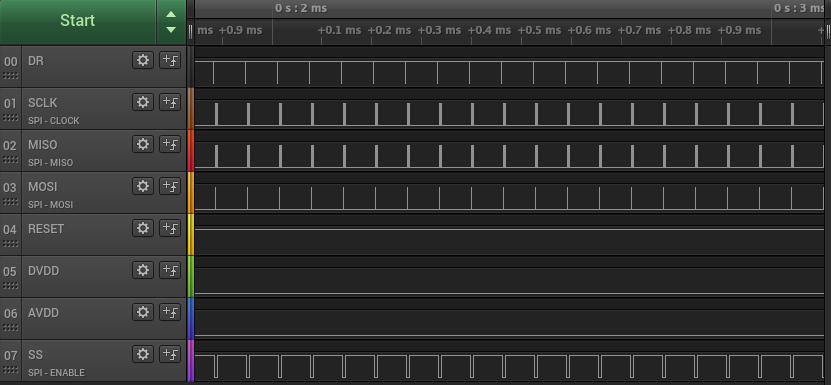
Two other issues that showed up was the fact that even at the highest PGA setting, low-current transients through the current amp quantize heavily and cause a lot of quantization noise, effectively imposing a bandwidth limitation, as the quantized signal needs to be filtered to remove the high frequency components which make up its hard edges. I've solved this issue by increasing the transmitted data length from 16 bits to 24 bits, which has caused yet another issue on the acquisition side. I had thought that at high frequencies the SPI would become an issue, but testing with the logic analyzer shows that the system is still capable of up to 125kHz data rate without issue on the SPI peripheral side of the system.
In increasing the throughput of data by a third, I've created a buffer overrun event when the acquisition code is formatting the input data into the ascii encoded decimal CSV format that for MATLAB. During the read loop, the rx buffer never gets to be larger than ~500 bytes, however, after the formatting, and crc calculation, the rx buffer size is routinely over 4000 bytes, which is larger than the internal tx buffer in the ft2232h, causing data corruption. I've added wait-states to the PMP transaction to decrease the reliance on low-latency reading (possible as there's lots of wiggle room in the acquire-transmit delay), but that's no way to solve the issue, and only acts as a small optimization. Moving to linux-rt doesn't solve the issue either, as the problem doesn't lie in I/O latency, but rather in the order in which things happen.
To solve this issue, and to make it more robust at higher data-rates, I've elected to implement a solution which uses multi-threading such that the FIFO can continuously be read, even while formatting and writing the data to the disk. Luckily I've thought ahead and built the system to use timeouts and the select() function to hopefully make threading easier.
Here's a nice short-time fourier transform of the spectral power density of the current harmonics of a lamp, and a solder fume fan being turned on and off:
Now that I've convinced myself that the data coming from the DAQ is not-corrupted, I've been able to start testing the data in MATLAB to see if the MCP3912 is behaving properly in regards to expected vs. actual spectral energy distribution for known signals. Apart from small offset errors, everything seems to look correct.
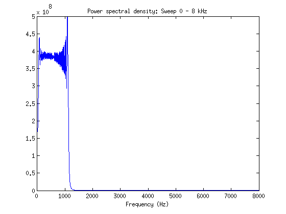 Out of curiosity I decided to take off the anti-aliasing filter to see what white-ish noise looks like with aliasing on the MCP3912.

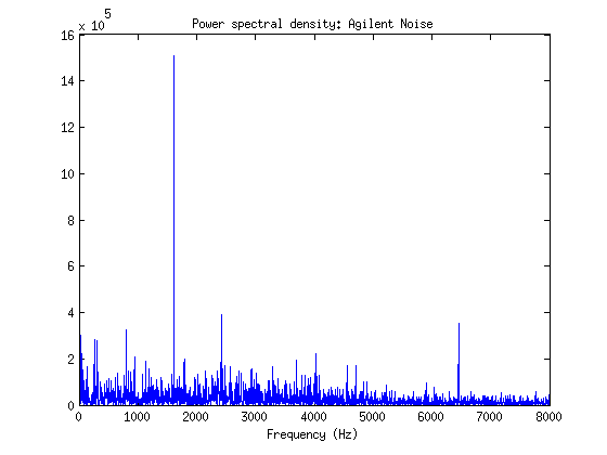

Everything seems to look correct, even with the impedance matching resistors on the SPI line removed. I'd like to hook up the agilent arbitrary function generator to the spectrum analyser to determine just how normally distributed the noise really is before I say that everything on the MCP3912 is working perfectly. Even though the DAQ is really well protected against cross-talk and ground bouncing, I'd like to see how much different the distribution of noise becomes with the impedance matching resistors added back into the system.
I've moved away from using the VCP libraries on the acquisition side of the DAQ to remove the reliance on kernel specific usbserial and ftdi_sio modules. The new acquisition script turns off those modules, and uses the cross platform D2XX library which gives direct access to the FT2232H device over serial, removing the complicated mess of configuration and debugging required with the virtual com-port drivers. Additionally, this shift has allowed me to move over to the byte wide FIFO that I connected to the PMP on the PIC32. With the PMP/DMA and the FT2232H, I've bumped up the tested throughput to 20 MByte/s with headroom to spare (even with the CRC calculations included).
Now, the biggest bottleneck with the pic32 and the AFE on the pants board is the 20MHz spi clock. With this dramatic increase in speed that the FIFO adds to the system the just-in-time CRC calculation that I was doing earlier doesn't complete in time to be appended to the FIFO's transmit buffer before the transaction is completed. Now that I'm not limited in bandwidth as I was before with the UART module, I've moved the PMP transaction initialization to the DMA CRC interrupt such that the PMP transfers all 18008 bytes in the buffer as soon as the DMA channel computing the CRC completes its CCITT calculation. As it stands, the only thing that needs to be reworked with the D2XX library is a better transmission system for starting and stopping transactions. My next order of business is to take care of the initialization and termination of acquisition through UART and the state-machine callback function in the UART DMA RX channel.
Analysis of the UART based acquisition with CRC's is showing that there is enough data corruption at the baud-rates that I'm working with to warrant continuing development on the FIFO based acquisition system with PMP on the pic32 and the FT2232H's FIFO channel.
When we start to use our DAQ for signature generation, the integrity of the data that we collect is going to need to be trusted. Toward this goal I've set up two spare DMA channels to compute the Standard CCITT CRC with polynomial: X^16+X^12+X^5+1, hex=0x00011021. This is computed as soon as the block begins to transfer, and the result is appended to the block to be transferred and compared on the receiving side. As all of this is done through the DMA engine, it requires minimal CPU overhead (some interrupt handling).
The new XC32 compiler has some interesting problems with backward compatibility. A lot of the provided macros and #defined interrupt vector values have been changed, with some aliases added, and others removed. While _DMAx_VECTOR exists for 0-3, 4-7 aren't redefined, but can still be written as _DMA_4_VECTOR. The raw vector numbers are 36-43, and I've elected to just use those with proper documentation nearby as using these doesn't throw any compiler warnings about backward compatibility.
Now that the DAQ is properly sending and receiving data, I now need to focus my efforts on ensuring that the data is stored and captured in a way which yields itself well for processing on the BBB. As we're most likely going to be using threaded processes, the data acquisition component of this project needs to be thread-safe and non-blocking.
Setting up the serial port as a socket and reading from it only when select() indicates that there's data to be read from the rx buffer should help to reduce the amount of cpu overhead that the serial link data transfer from the DAQ introduces.
As the FTDI chip supports non-standard baud-rates to the linux/serial and ioctl libraries, I need to not only set up the script to handle threading correctly, but to properly prescale the reported base baudrate of the ft2232 to drop it down from 60MBaud down to whatever it is that I'm using to read from the DAQ. For testing purposes I've set it to (2MBaud).
Additionally, I've been considering using the built-in CRC checksum feature that the DMA engine on the PIC32 has to ensure that the data blocks transferred are received properly by the BBB. Relying on the CRC would allow me to make assumptions on the form of the data, as deviations in the form due to corruption during transmission would show up when looking at the CRC at the end of the transfer.
ToDo:
- Thread-safe socket-based serial device aquisition. (Priority 1)
- Implement CRC on both receive and transmission side of the DAQ to ensure no data is lost. All zero block in the event of a corrupted value.
As a precursor to high-speed FIFO acquisition, uart needs to work. Now that I have the ADC sampling at its maximum rate, I can slow down the sample rate to test the acquisition to a PC over USB.
There were a few issues with the order in which SPI and the MCP initialization code was run which caused some interrupt flags to never be handled properly, causing inconsistent data acquisition and transmission. Setting SPI1STAT to zero at the beginning of each DMA SPI RX request solves this issue and allows it to be initialized anywhere after the SPI peripheral is brought up in the code.
With UART_ENABLE_HIGH_SPEED disabled the fastest baudrate that the PIC32 can handle is 1,152,000. With the BRGH bit set we can max out the default linux 3.13.0-44-generic FT2232 driver baud rate of 4MBaud. With UART, a cursory analysis reveals that we're able to acquire data at up to 64 kHz with four channels without any optimizations. With proper optimizations we may be able to get away with using just UART and no FIFO for these speeds. A proper investigation will most undoubtedly reveal that the FIFO will have less data corruption, but as we only really need a sample rate of 16 kHz, I'll put it on the back-burner for future work.
While I'm knee deep in DMA, I'm going to make sure that we have a way of controlling the DAQ with UART, so that we can start and stop acquisition with the ESP module. I'll have the DMA RX fire off an interrupt on a pattern match of \r\n as that's the termination for the AT commands on the ESP module as well as for our NMEA-like protocol for data.
As was already established on 1/10/2015 the SPI TX complete flag which is used along with the DMA transfer complete flag corresponds to the completion of data being shifted into the SPI FIFO for transmission, but doesn't indicate that the system has transmitted out the entire byte of data. With DMA working on the RX channel, the delays added during initialization are unnecessary as I've moved from doing a register-by-register write/read to bulk reads which reduces the amount of CS toggles, and the need for extra delay after transactions.
Notes:
- Letting DMA handle interrupt requests from the SPI peripheral has a lower latency than handling them with user-defined isr routines, e.g.
__ISR(_CHANGE_NOTICE_VECTOR)
As of right now we have a system which samples data from the MCP3912 and transfers it over DMA to the PMP with minimal interaction from the CPU core. Using a timer and a counter to measure idle clock cycles I've measured an overall CPU utilization with the current set-up as 5%, which is comprised of the code being run in the Change Notify interrupt, and the DMA2_CHANNEL buffer switching interrupt.
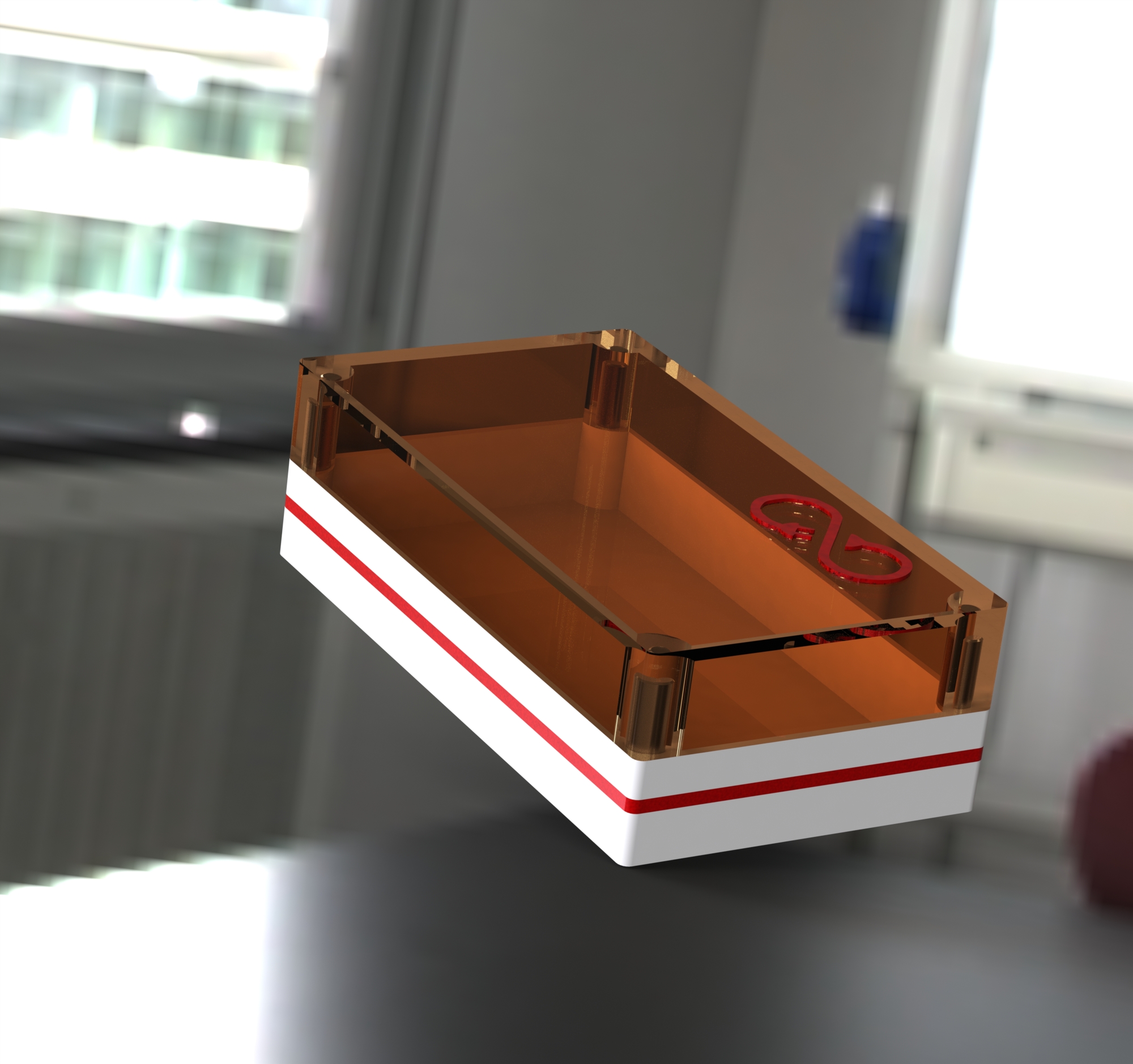
Our partner in industry has requested a 3D representation of what I might think the end result would look like. This has spurred me to make a quick render of our rough assembly sizing so that I can think about how I'm going to stack PCB's and fit the appropriate connectors / AC/DC conversion hardware. Having a 3D CAD version of this to work with is going to allow me to better understand the constraints on the electrical design due to thermal resistance of the case, TDP of the components, and the limitations on volume.
SPI RX with DMA is now working correctly and apparently always was. The script I wrote in MPLAB to check the integrity of the data I was receiving didn't take into account the fact that the MCP3912 also sends out its configuration data during the initialization routine. Now that this mystery is solved I can move forward. I've added a function which enables the SPI RX separately from the SPI TX DMA channels and I am now initializing it after I finish and confirm the setup of the MCP3912.
I've tracked down the problem with SPI configuration down to endianess. Rather than writing in a byte by byte endianess swapper in the configuration data code, I'm going to rewrite the typedefs which describe the bit-fields for the configuration registers. Since not all configuration code is byte aligned this is one of the more straight-forward solutions. NOTE: Fixed.
With a clock pre-scaler of 1 and oversampling ratio of 32 (0b000), I've confirmed a sample rate of 125 kHz for four simultaneous channels.
The external crystal oscillator seems to be working and using it as the internal clock source has gotten rid of missed change notification events and the previous limitation on the maximum SPI clock rate. There's still something funky about the
while (!(DmaChnGetEvFlags(DMA_CHANNEL1) & DMA_EV_BLOCK_DONE) || !(SpiChnTxBuffEmpty(SPI_CHANNEL1)));
call used to signify the end of a conversion. It's always a little too early. I fixed it by adding some junk additions after it (Nop()'s don't work), and in practice this shouldn't be a problem as there is always going to be at least a single function call after checking for the end of the block transfer, so I'm going to tentatively say that this is a non-issue outside of initial configuration timing.
As the current configuration stands, there is a combined interrupt and system delay of 3uS between the DR pulse and the start of the SPI result transfer. Every 16 bit value takes about 1uS to shift out of the AFE which means that at the maximum SPI frequency, the system can transfer all four channels to the pic in a span of 6-7uS. That should tentatively put us in the ballpark of a maximum sample rate of 140~kHz, which is higher than the maximum rated speed of the analog front end. (Using 1/f)
Unfortunately it looks like we'll only be able to reliably sample the ADC at a rate of ~66 kHz as with DMA and some optimization, we're /just barely/ able to complete 4 transfers at the maximum sample rate of 4 MHz.
the DMA code:
DmaChnClrEvFlags(DMA_CHANNEL1, DMA_EV_BLOCK_DONE); DmaChnSetTxfer(DMA_CHANNEL1, adcBuf, (void*) &SPI1BUF, 13, 1, 1); DmaChnSetEvEnableFlags(DMA_CHANNEL1, DMA_EV_BLOCK_DONE); DmaChnStartTxfer(DMA_CHANNEL1, DMA_WAIT_NOT, 0);
was placed inside of the SPI_Read_Result_Registers function to reduce the amount of cycles wasted on function calls. With that change and some other code repositioning I was able to make timing, but I'm not sure that there's much more room to speed it up without destroying the modularity of the code. At least with how it stands now we'll have plenty of overhead to do other operations at lower sample rates.
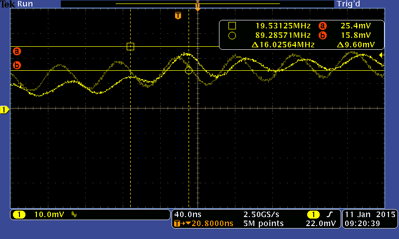
The oscillator output to the MCP3912 captured on the DPO 3054. Apparently the print screen operation messes with the averaging function, next time I'll make sure to stop the capture process before printing the screen. 👎
The DMA RX channel is being set up to transfer data into an address and increment the memory pointer after every received byte from the mcp3912 up until it has filled up the entire 8192 bytes in the destination address. Once the destination is full it will trigger an interrupt where I can then reconfigure the DMA RX channel to spit data into the second buffer while the data in buffer 1 gets sent over UART or eventually the USB FIFO.
Some Notes:
- SPI1 and SPI1A are not the same.
- Getting DMA to work with SPI RX is painful.
Both AVDD and DVDD to the AFE pants come up at the correct times, and all of the level sensitive inputs check out. The startup delay is appropriate, and the spi data checks out with the logic analyzer. The default device address bits are A<7:6> = 01 whereas in the control bit right now I'm using 00. An |= 0x40 with the control byte should fix this. NOTE: It did fix it.
When initially reading from the device we see that the configuration registers correspond to the correct POR initial values. However, after writing to the registers we see that only some bits are set while others are not. Moving from the logic analyser to to the oscilloscope should yield some more information about the integrity of the SPI lines at 4 MHz.
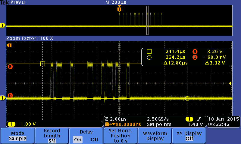
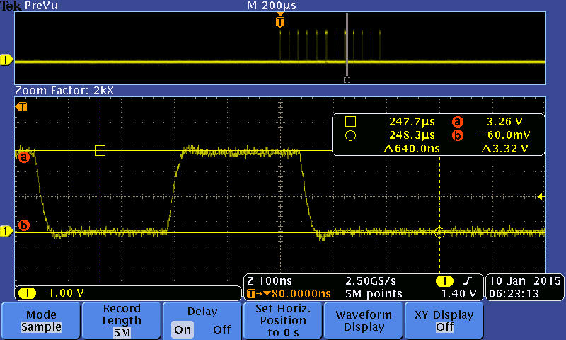
These scope traces would suggest that the integrity of the MOSI line is not the problem. I'm going to attempt to bulk write and read from the configuration registers to see if the problem persists with that configuration.
Many of the outputs of the MCP3912 are high-impedance when they aren't being used. Two in particular are the DR (data ready) pin and the SDO from the device when it isn't transmitting anything. As a result, capacitive and inductive reverse coupling are quite evident.
- The interboard connector should have two ground pins between each signal in the next pcb boardrun to reduce crosstalk. In the short term, a weak pull-down can be added to DR, MISO does not have CN functionality and therefore doesn't have a built-in pull-down. These correspond to pins 49 (RF4 -- DR) and 9 (RC4 -- MISO). For now all of the crosstalk has a swing of +/- 20mV, which is perfectly acceptable at this point. If data integrity becomes an issue after the addition of more ground isolation in the IBC, then I should revisit this.
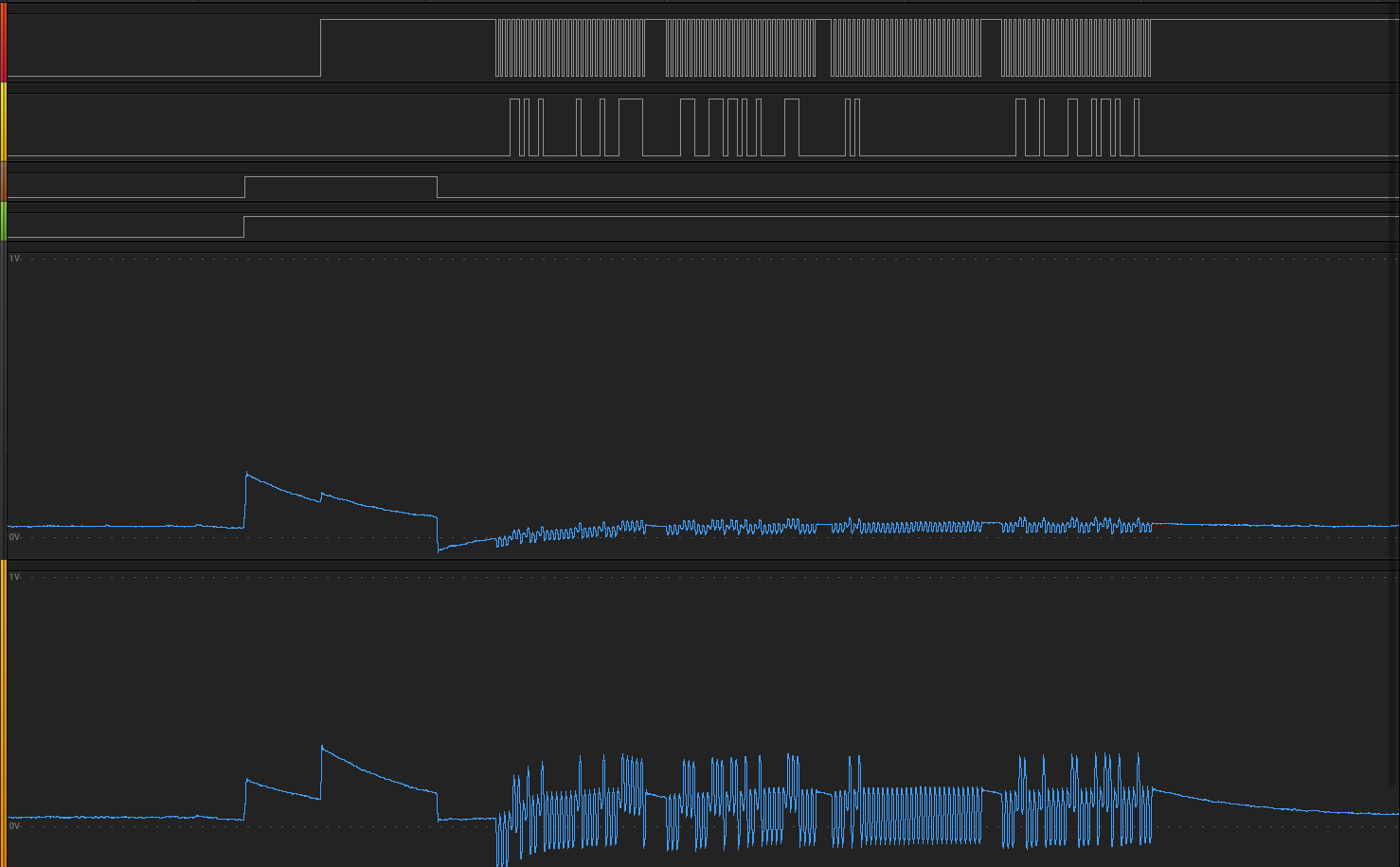
DMA's interrupt flag DMA_EV_BLOCK_DONE and the completion of the SPI transmission don't seem to coincide. There are three clock edges that are missed as DMA_EV_BLOCK_DONE goes high when the SPI module is 3 bits away from completing the shift out onto MOSI. The errata doesn't seem to show anything regarding the DMA or the SPI which mentions this, so I may look to check for both DMA_EV_BLOCK_DONE and some sort of SPI transmit complete bit.
while (!(DmaChnGetEvFlags(DMA_CHANNEL1) & DMA_EV_BLOCK_DONE) || !(SpiChnTxBuffEmpty(SPI_CHANNEL1))); SPI_SS_LAT = 1
That snippet solves the problem.
After changing an LP2989 on the AFE pants board, the system now has both the analog and digital 3.3v supplies reaching the IC. No response is being given from the device. Things to check:
- Adequate start-up delay?
- Double check integrity/correctness of responses
- Check that the external oscillator is in fact oscillating.
In the MCP391x library I'm using settings which correspond to a sample rate which is around 16kHz. Most of the bit-fields are well documented in the header, anything mentioned below is done so with the assumption that they may be sources of error during debugging.
-
The boost bits in CONFIG 0 is set to 0b11 which corresponds to a current bias of 2x. This supposedly affects the sample rate, but it is a little unclear as to how. Table 5-2 in the MCP3912 datasheet has all pertinent information regarding that.
-
OSR and PRE are pretty straightforward.
-
The sample-rate of the device is MCLK/PRE/OSR. In this case we have 16MHz / 8 / 128 = 15.625 kHz.
-
VREFCAL, OFFCAL and GAINCAL all change the overall accuracy of the current measurements made by the MCP3912. VREFCAL trims the internal VREF to deal with drift over time due to temperature variations. We probably don't need to deal with this right now, but it would be smart to revisit this once we have basic overall functionality. GAINCAL adds a gain offset to the sampled data and introduces a system delay as it takes a few clock cycles to multiply the calibrated constant. OFFCAL introduces an offset and does not introduce any system delays.
-
RESET and SHUTDOWN are on a channel by channel basis and put the channel into a soft-reset or on/off mode. 0b0001 corresponds to channel 0 while 0b1000 corresponds to channel 3.
-
PHASEA/B are used for ensuring proper phase delay in the SINC filter outputs, we will need to look at this, but only when we start to do analysis of power signatures.
-
WIDTH_DATA is currently set to 0, which sets up all result registers to be 16 bits wide and rounds all data to this width.
-
The data ready pin goes from logic high when data is not ready to high-z when it is ready. This means that I'll need to use a weak pull-down on the pin that it's connected to on the pic. With the weak pull down, a data ready event should be represented by a falling edge on the DR pin.
-
STATUS.WRITE sets up continuous writing settings. Initially I'm just going to write one register at a time with a chip-select toggle between each one for debugging, but this should be changed such that on start-up the entire set of configuration data is written to the device.
The MCP3912 works with SPI modes 0,0 and 1,1. This means that on the pic, SPI mode 0,0 has CKP = 0 and CKE = 1. SPI mode 1,1 has CKP = 1 and CKE = 0. In more standard terms this is expressed as SCK's polarity and SCK's phase as both either being 0 or 1.
In mode 0,0: 0 = Clock Idle low level, 0 = SDO transmit edge (*) active to idle In mode 1,1: 1 = Clock Idle high level, 1 = SDO transmit edge idle to active
MISO data should be sampled on the rising edge of SCLK as SDO of the MCP3912 latches on the falling edge, this will give adequate time for ringing to settle.
The multi-purpose connector has a whole bunch of peripherals broken out on it and I've elected to use some of the unused ones as digital IO for the MCP3912. They are as follows:
NOTE: SIWUA pin on the ft2232 adapter is currently floating on DAQ board v2.0b, and should be connected to VCCIO as it is unused. A pin next to it has 3.3v on it and should be shorted to the SIWUA pin in this revision if there are any data transmissions problems (they haven't shown up yet.)
