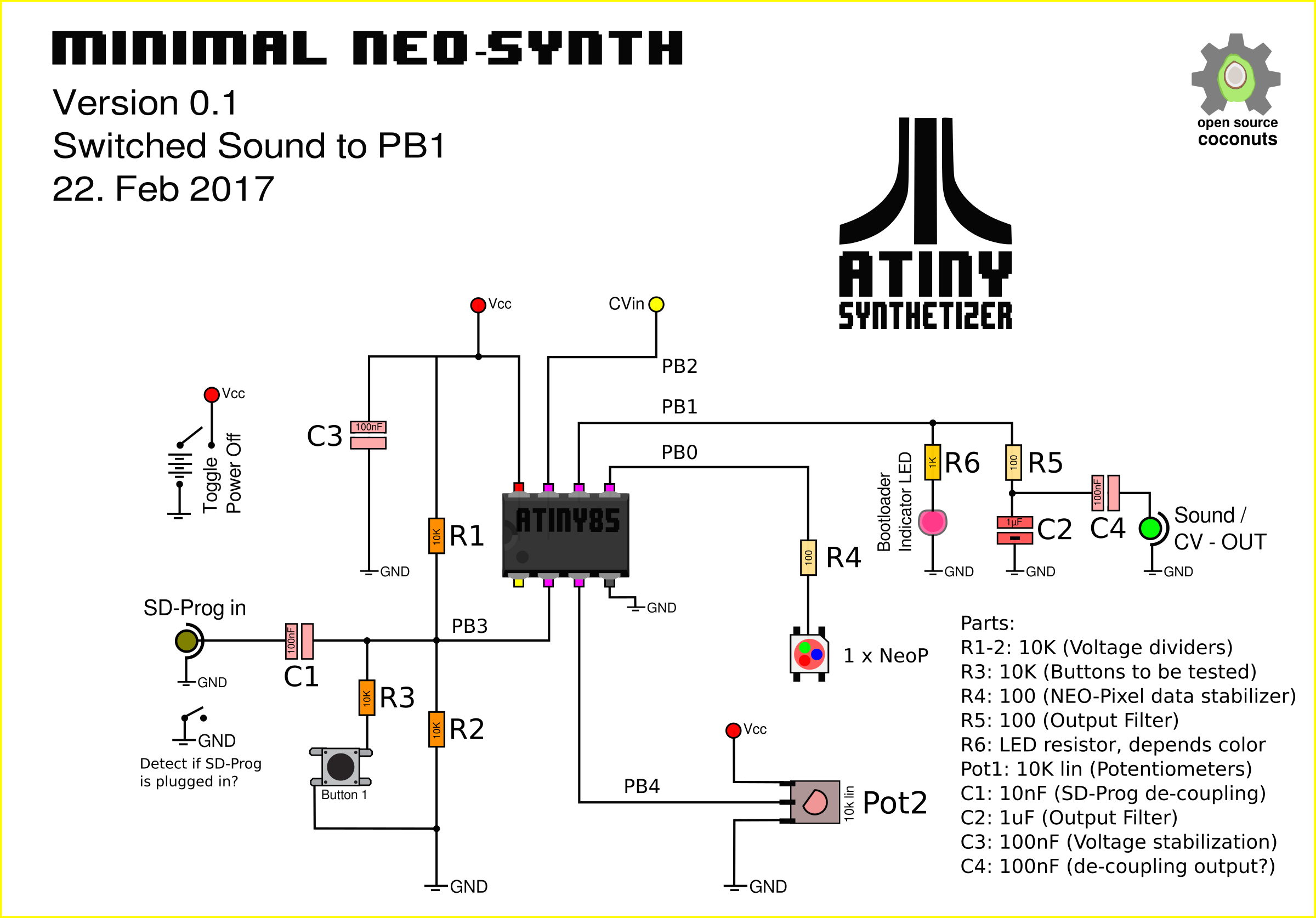
4_2 Schematics Discussion
how to free even more pins on that little attiny85...

![]()
More minor improvements, suggested by Uwe:
- Add CV In 2 (cos we can)
- No decoupling cap, or CV out is wrong
- That thing with the switch on the Sound-prog jack.... ?
- What kinda swtiched jack-socket is that?
![]()

Parts:
- R1-4: 10K (Voltage dividers)
- R5: 10K (Buttons to be tested)
- R6: 4K7 (Buttons to be tested)
- R7: 100 (NEO-Pixel data stabilizer)
- R8: 100 (Output Filter)
- R9-10: LED resistor (depends on color)
- Pot1-2: 10K lin (Potentiometers)
- C1: 100nF (SD-Prog de-coupling)
- C2: 1uF (Output Filter)
- C3: 100nF (Voltage stabilization)
- C4: 100nF (de-coupling output?)
Pin Use:
- PB0(pin5): NEO-pixels
- PB1(pin6): Sound output (parallel LED)
- PB2(pin7): (A1) Potentiometer (right), CV input
- PB3(pin2): (A3) Buttons/Switch via Voltage-Dividers
- PB4(pin3): (A2) Potentiometer (left), SD-Prog Jack-3.5mm Input
- PB5(pin1): (A0 )kinda free pin, can be used for sync / gate signal and communication from the bootloader
- GND(pin4):
- Vcc(pin8): Power LED, stabilizing cap Vcc-GND.

Still confused about the possibility to detect if the mini-jack is plugged using the "normally connected" part of the jack-socket?

Parts:
- R1-4: 10K (Voltage dividers)
- R5: 22K (Buttons to be tested)
- R6: 47K (Buttons to be tested)
- R7: 100 (NEO-Pixel data stabilizer)
- R8: 100 (Output Filter)
- Pot1-2: 10K lin (Potentiometers)
- C1: 100nF (SD-Prog de-coupling)
- C2: 1uF (Output Filter)
- C3: 100nF (Voltage stabilization)
- C4: 100nF (de-coupling output?)
Pin Use:
- PB0(pin5): Sound output (parallel LED)
- PB1(pin6): NEO-pixels
- PB2(pin7): (A1) Potentiometer (right), CV input
- PB3(pin2): (A3) Buttons/Switch via Voltage-Dividers
- PB4(pin3): (A2) Potentiometer (left), SD-Prog Jack-3.5mm Input
- PB5(pin1): (A0 )kinda free pin, can be used for sync / gate signal and communication from the bootloader
- GND(pin4):
- Vcc(pin8): Power LED, stabilizing cap Vcc-GND.

Parts:
- R1-5: 10K (Voltage dividers)
- R6: 4K7 (Voltage dividers)
- R7: 100 (NEO-Pixel data stabilizer)
- R8: 100 (Output Filter)
- Pot1-2: 10K lin (Potentiometers)
- C1: 100nF (SD-Prog de-coupling)
- C2: 1uF (Output Filter)
- C3: 100nF (Voltage stabilization)

Others: Do we need extra caps for the NEO-pixels?
Interface:
- 2 potentiometers
- 2 push-buttons
- 1 Sound output PWM (PB0 is preferred) is also CV output in case of Sequencer code
- Sound-progger input
- CV input
- Master-clock or gate output
- Sync-clock input
- 1 pin to communicate wiht the 8 NEO-pixels (is that cheating?)
- what else?