-
Notifications
You must be signed in to change notification settings - Fork 43
Usage
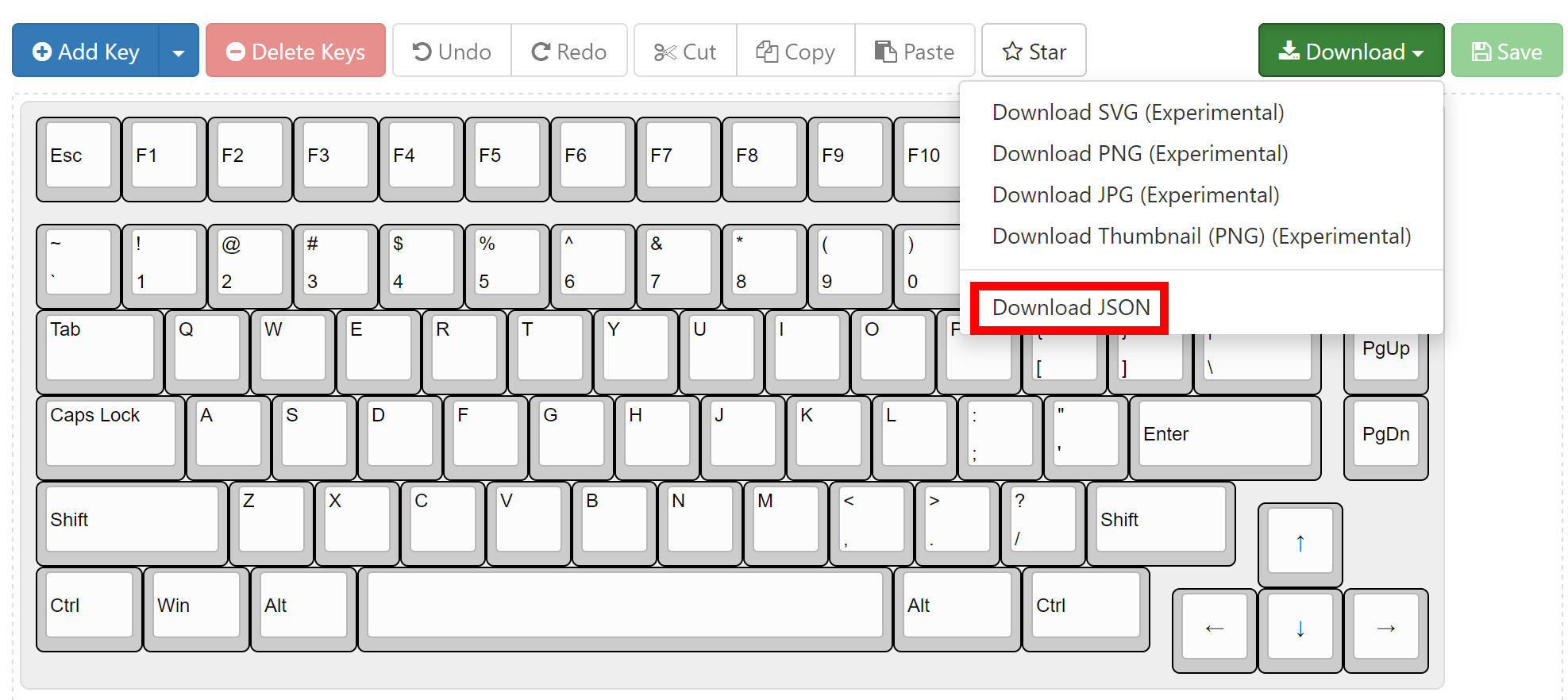
First order of business is to generate the base Kicad project. For this you need to download the JSON file describing a keyboard layout from the Keyboard Layout Editor using the download button:

Next, execute the script from the commandline with the necessary options. Using the provided example keyboard layout looks like this:
python klepcbgen.py -o mykeyboard example_layout.json
The script reads the layout described in "example_layout.json" and generates a KiCad project in the subdirectory "mykeyboard"
While klepcbgen takes care of most of the tedious and error-prone drudge-work, it cannot generate a finished design you can immediately send off to be manufactured. There are a few manual steps required to get everything in working order. First, you need to properly link the schematic and layout and update the footprints:
- Load the project in KiCad and double-click the kicad_pcb file to open it.
- From the Tools menu, select Update Footprints from Library...
- Make sure Update all footprints on board is the selected option, then click Apply. Once it finishes the update, click Close
- From the Tools menu, select Update PCB from Schematic...
- This will open the Annotate dialog for the schematic. Ensure Keep existing annotations is selected, then click Annotate
- KiCad will automatically switch back to the Update PCB from Schematic... dialog once it finishes the annotation
- Ensure the Match Method is set to Re-associate footprints by reference (for Kicad 5) or Re-link footprints to schematic symbols based on their reference designators (for Kicad 6). In both cases THIS IS NOT THE DEFAULT, so be sure to change it or it will mess up the switch placement.
- Click Update PCB
The schematic and pcb layout are now properly linked, but the layout is not yet finished.
The script tries to partly route the key matrix. For this it applies some simple heuristics which give usable results in most cases. However, there's a chance this simple approach leads to issues you'll need to fix, such as shorts or traces interfering with pads or through-holes.
- Run the Design Rule Checker (Inspect -> Design Rules Checker -> Run DRC).
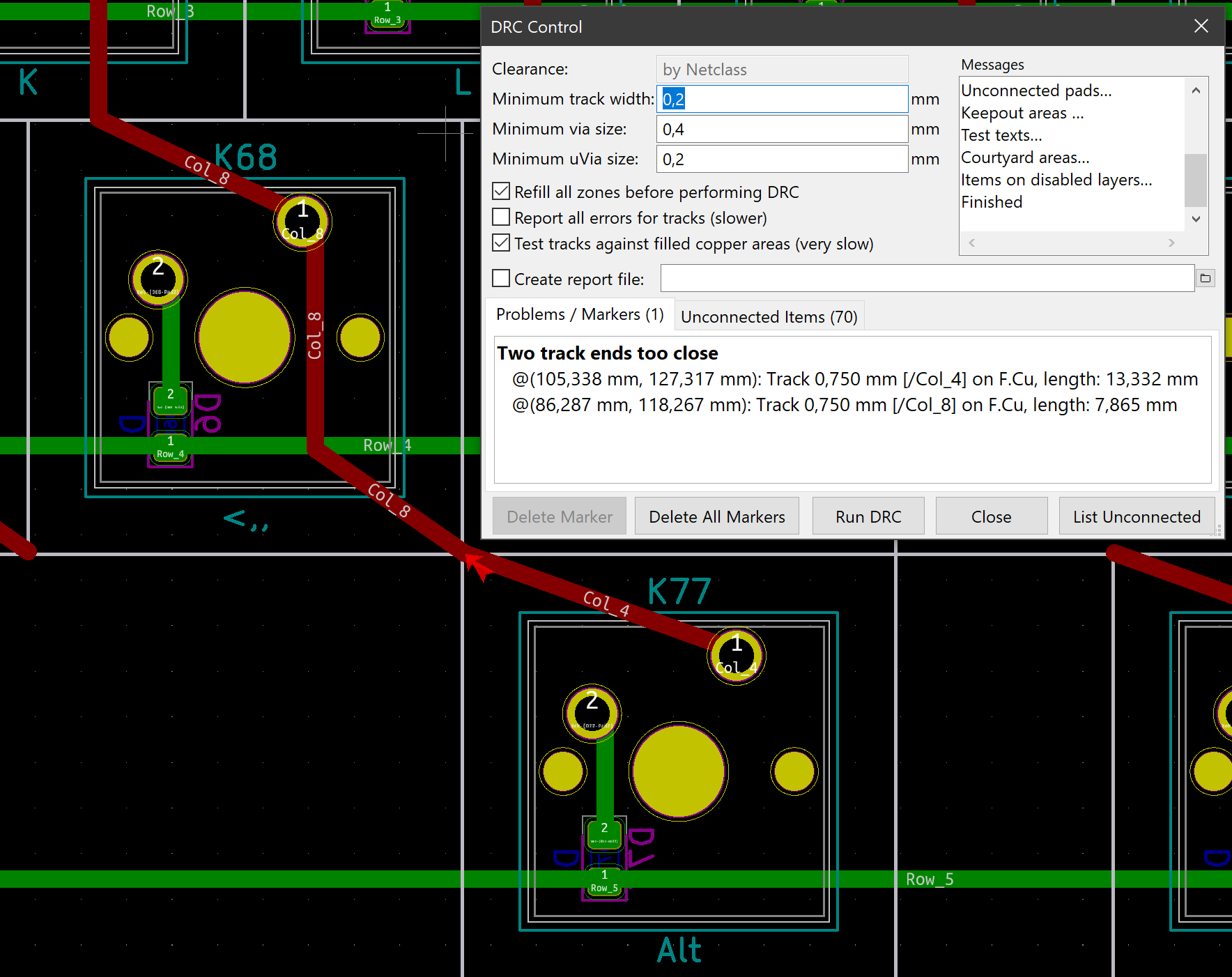
- Check and fix any issues found in the "Problems/Markers" report (disregard the unconnected items for now). This can look something like this:

In this case, the up-going trace from K77, which is in Column 4, touches the down-going trace from K68, which is in Column 8. Delete one or both of the traces and redo the connection in the following step
Next you need to finish the layout, since there are still a lot of unconnected traces. Automatically routing these connections is beyond the scope of this script, so the next step is finishing the board layout manually.
- Place the microcontroller circuit and USB connector. The best spot for these is highly board-specific and depends on personal preference.
- The script adds traces up to the boundary of each switch footprint. Sometimes this succesfully connects a switch to the next one in the column, but it often doesn't, so you'll have to make this connection yourself.
- Connect the key-matrix and USB connector to the control circuit. This is the most time-consuming step as you will quickly run out of space in the area around the microcontroller.
Once you finish the PCB, you can generate the set of Gerber files, as explained for example in this guide.