-
Notifications
You must be signed in to change notification settings - Fork 8
PLLs Advanced
In the PLLs Improved article, we already talked about the different PLL primitives that are listed in the ICE Technology Library.
Let's now go deeper into that.
-
SB_PLL40_CORE
The SB_PLL40_CORE primitive should be used when the source clock of the PLL is driven by FPGA routing...
The simplest kind of PLL. Can be used universally. But we now know that it's usually not the best choice for the BlackIce-II board.
-
SB_PLL40_PAD
The SB_PLL40_PAD primitive should be used when the source clock of the PLL is driven by an input pad ... and the source clock is not required inside the FPGA.
Perfect for your simple programmable clock needs!
-
SB_PLL40_2_PAD
The SB_PLL40_2_PAD primitive should be used when the source clock of the PLL is driven by an input pad ... and in addition to the PLL output, the source clock is also required inside the FPGA.
Remember how we could not use the input from an IO pad in which a PLL also used? Well... it's possible after all!
-
SB_PLL40_2F_CORE
The SB_PLL40_2F_CORE primitive should be used when PLL is used to generate 2 different output frequencies, and the source clock of the PLL is driven by FPGA routing i.e. when the PLL source clock originates on the FPGA.
Two different output frequencies from one PLL? That sounds interesting...
-
SB_PLL40_2F_PAD
The SB_PLL40_2F_PAD primitive should be used when the PLL is used to generate 2 different output frequencies, and the source clock of the PLL is driven by an input pad
Even more interesting!
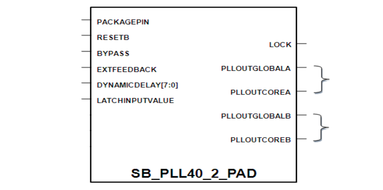
Here's a diagram with the IOs of this PLL primitive:

We see the same IOs as for earlier PLLs, except for the fact that there are now 2 sets of outputs: A and B.
This PLL primitive behaves exactly the same as SB_PLL40_2_PAD except that PLLOUTGLOBALA and PLLOUTCOREA
contain a copy of PACKAGEPIN, while PLLOUTGLOBALB and PLLOUTCOREB have the new clock that is generated
by the PLL.
Check out the sb_pll40_2_pad_global example.
After running this, you shold see the red LED blinking about 3 times
faster than the orange LED, just like our very first PLL
example.
The only difference is that, this time, we have a straight connection from the CLK_OSC100 pin to the PLL that's right next to it.
Note: In the example, we are using the GLOBAL outputs instead of CORE. Not only is this the optimal way of doing things,
it's also the only way to get this example to work. For some reason, PLLOUTCOREB does NOT have
the expected clock, and the orange LED doesn't blink.
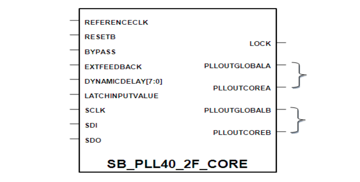
The diagram with the IOs of this PLL primitive:

This looks... underwhelming. It's basically the same as the one before, except for having a REFERENCECLK
instead of PACKACKEPIN.
But let's not forget about the promise from the Technology Library:
The SB_PLL40_2F_CORE primitive should be used when PLL is used to generate 2 different output frequencies, and the source clock of the PLL is driven by FPGA routing i.e. when the PLL source clock originates on the FPGA.
Unfortunately, this oversells the capabilities. There is only one VCO per PLL, so the only possible way to
generate multiple frequencies is by having multiple output dividers. But it's not even that. The only way
you can create a different frequency is by assigning a value of "GENCLK_HALF" to the
PLLOUT_SELECT_PORTA or PLLOUT_SELECT_PORTB parameter. And when you do so, that output port will
carry a clock that is exactly 50% of the normal frequency.
The sb_pll40_2f_core_global example shows how that works.
In pll.v, you see the following extra line:
.PLLOUT_SELECT_PORTB("GENCLK_HALF")
When you run this example on your board, LED1 (red) will blink using the fastest, 100MHz, clock that comes straight
from the CLK_OSC100 pin. LED2 (orange) blinks 3 times slower, using a 30MHz clock. And LED3 (green) blinks another
50% slower because thanks to the "GENCLK_HALF" parameter, its blinking circuit only uses a 15MHz clock.
This primitive is similar to the SB_PLL40_2F_CORE, but it uses a package pin as input instead of a regular internal routing net.
Here's the example: sb_pll40_2f_pad_global.
This is where everything comes together!
The dual_pll_4clocks has 4 LEDs blinking at different clock speeds.
- LED1 (red) uses the 100MHz input clock. Since we want to use the PLL that is part of that same IO, we have to use an SB_PLL_2_PAD primitive, and use the PLLOUTGLOBALA output.
- LED2 (orange) uses a 30MHz clock that is generated by the top PLL.
- LED3 (green) uses a 25MHz clock that is generated by the bottom PLL. The bottom PLL is of the SB_PLL_2F_CORE type and also uses the 100MHz clock as input.
- LED4 (blue) uses a 12.5MHz clock, also generated by the bottom PLL.