-
Notifications
You must be signed in to change notification settings - Fork 8
PLLs
The BlackIce-II board has a 100 MHz oscillator that feeds straight into the FPGA.
Very often, we want to run part or all of our logic at a different clock speed.
This is where PLLs (Phase Locked Loop) enter the picture. It's a fundamental building block, present is most chips of some complexity, that can be configured to generate a clock with a wide range of frequencies.
The ICE40 HX4K FPGA on your board has 2 such PLLs.
Feel free to skip this section if you're not interested in the inner working of a PLL.
We can find a lot of PLL information in the Lattice iCE40 sysCLOCK PLL Design and Usage Guide and the ICE Technology Library.
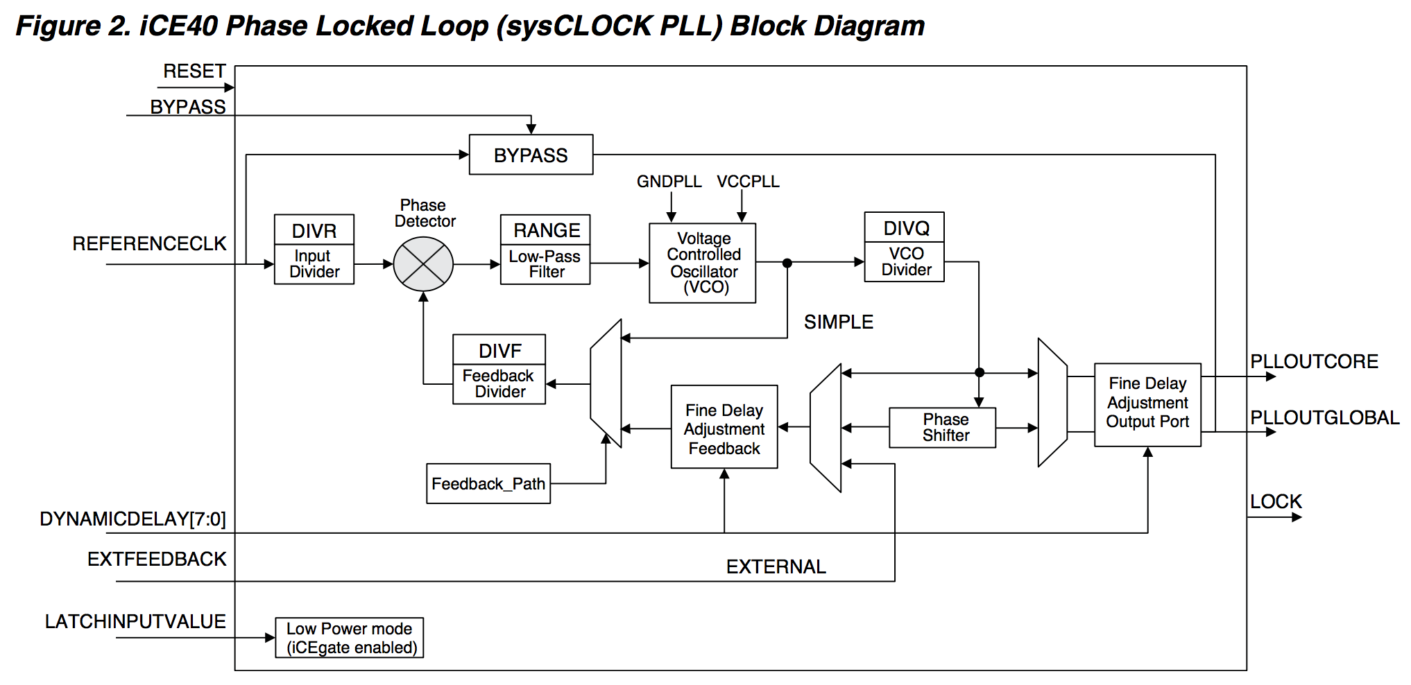
In the Design and Usage Guide, you'll see the following block diagram:

This can be a little overwhelming if you've never used a PLL before! FPGAs are versatile beasts with a lot of different applications. To ensure that most options are covered, FPGA PLLs often have a lot of advanced features that are not needed for day to day electronics where you just want to generate a different clock.
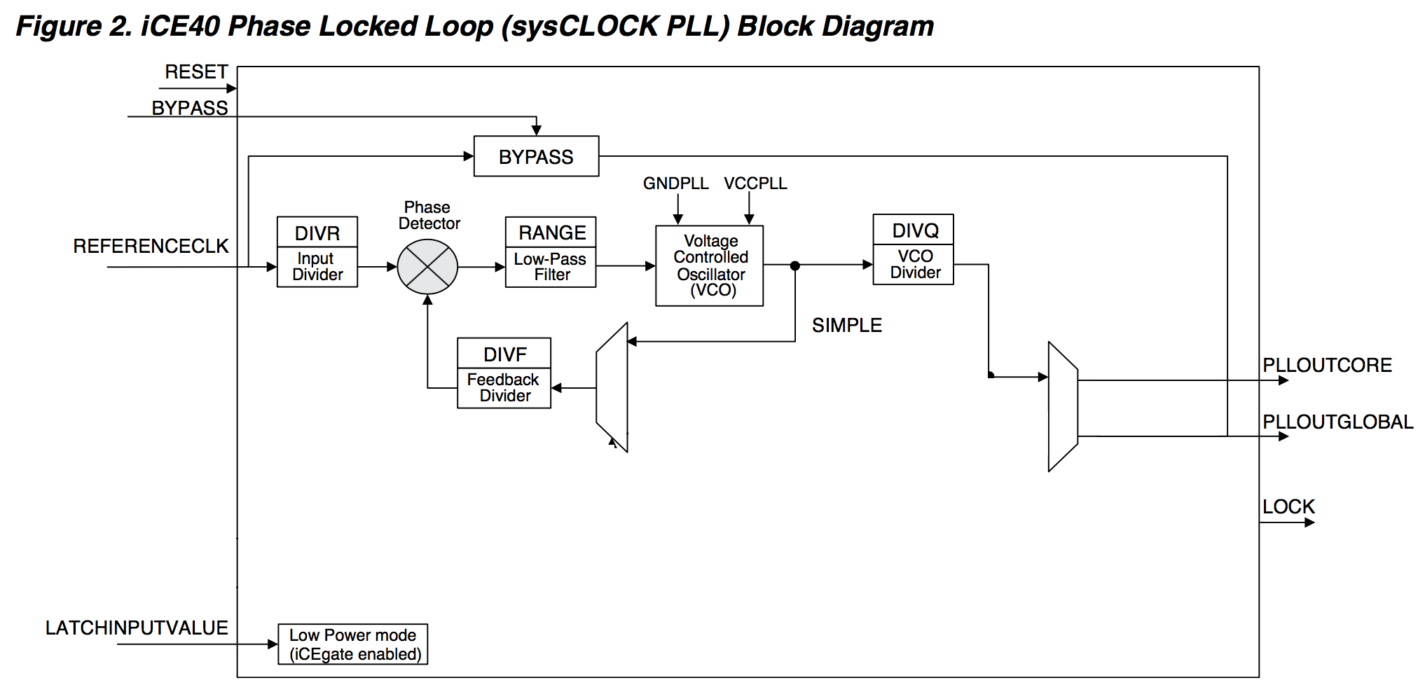
Lattice helpfully has a SIMPLE mode that reduces the PLL to something quite a bit, well..., simpler. Let's see what happens to the block diagram when we enable this mode:

A lot better! We're looking at a PLL that has been stripped to the bare minimum.
The most important part of an PLL is the voltage controller oscillator, or VCO. It's basically a clock generator that can operate over a large frequency range where the frequency is controlled by some internal voltage. In the case of our FPGA, the range of the VCO goes from 533MHz to 1066MHz.
That's much higher than what any reasonable digital circuit on an ICE40 FPGA could run at, but that's ok, because immediately
after the output of the VCO we see the VCO divider DIVQ. This block reduces the frequency of the VCO to something
much more reasonable: DIVQ can divide down by a factor of 2, 4, ..., 64. If the VCO were running at 533MHz with the divider set
to divide by 64, we'd get an output frequency of 8.2MHz. Similarly, running at 1033MHz and dividing by 2, we'd get 516MHz.
That's a very large range indeed!
What remains is how we actually control the VCO into generating these frequencies. For that, have the reference clock, an input divider, a feedback divider, and, most important, a phase detector.
In a closed loop from the phase detector through the VCO back via the feedback divider, the PLL tries to make sure that the frequency at the output of the input divider is identical to the frequency at the output of the feedback divider.
If we lower the reference clock or increase the divide ratio of the input divider (and thus lower the frequency of the signal that leaves the input divider), the VCO frequency will have to go down to make the output of the feedback divider match again.
However, if we increase the divide ratio of the feedback divider (and lower the frequency of the signal that leaves the feedback divider), the VCO frequency will have to up to make both frequencies match.
Putting everything together, this results in the following formula:

With that bit of theory behind us, how to apply this in practice?
The truth is: most of us don't really want to work with mathematical formulas. Given a certain input frequency, we want a desired output frequency and that is that.
Lattice has a set of tools for that, but we are married to the Project IceStorm open source software. Luckily, there is a basic tool that
provide just what we need: icepll. Given an input and output frequency, it create all parameters right there. If asked, it will
even create a Verilog file for you!
Let's try the following example:
icepll -i 100 -o 30
Results in the following:
F_PLLIN:   100.000 MHz (given)
F_PLLOUT:   30.000 MHz (requested)
F_PLLOUT:   30.000 MHz (achieved)

FEEDBACK: SIMPLE
F_PFD:   20.000 MHz
F_VCO:  960.000 MHz

DIVR:  4 (4'b0100)
DIVF: 47 (7'b0101111)
DIVQ:  5 (3'b101)

FILTER_RANGE: 2 (3'b010)
All the parameters that are needed to instantiate an ICE40 PLL is given. We also see that the requested output frequency, 30MHz, matches
the achieved frequency. This will not always be the case! In the previous section, we showed the forumula for the output frequency. It
depends on input frequency, and 3 divider settings. There are only a limited amount of divider settings, so not all output frequencies
can be generated. icepll will try to get as close as possible.
Here's an example of that:
icepll -i 100 -o 31
Gives:
F_PLLIN:   100.000 MHz (given)
F_PLLOUT:   31.000 MHz (requested)
F_PLLOUT:   30.938 MHz (achieved)

FEEDBACK: SIMPLE
F_PFD:   10.000 MHz
F_VCO:  990.000 MHz

DIVR:  9 (4'b1001)
DIVF: 98 (7'b1100010)
DIVQ:  5 (3'b101)

FILTER_RANGE: 1 (3'b001)
30.938MHz is pretty close to 31MHz, but it's not exact.
If you add the -f <verilog parameter file>, icepll will output just the Verilog parameters. They can be pasted into your
PLL verilog file. But if we add the -m option as well, we get a full functional Verilog mode for the PLL.
For example:
icepll -i 100 -o 30 -m -f pll.v
Creates the following pll.v file:
/**
 * PLL configuration
 *
 * This Verilog module was generated automatically
 * using the icepll tool from the IceStorm project.
 * Use at your own risk.
 *
 * Given input frequency:       100.000 MHz
 * Requested output frequency:   30.000 MHz
 * Achieved output frequency:    30.000 MHz
 */

module pll(
	input  clock_in,
	output clock_out,
	output locked
	);

SB_PLL40_CORE #(
		.FEEDBACK_PATH("SIMPLE"),
		.DIVR(4'b0100),		// DIVR =  4
		.DIVF(7'b0101111),	// DIVF = 47
		.DIVQ(3'b101),		// DIVQ =  5
		.FILTER_RANGE(3'b010)	// FILTER_RANGE = 2
	) uut (
		.LOCK(locked),
		.RESETB(1'b1),
		.BYPASS(1'b0),
		.REFERENCECLK(clock_in),
		.PLLOUTCORE(clock_out)
		);

endmodule
All we need to do now, is instantiate the pll module into our design. Wire up the clock_in input to our 100MHz oscillator input,
and use the clock_out output to drive our logic at 30MHz.
The chip.v of the PLL example does exactly that.
Things don't stop here though. Check out PLLs Improved to make things even better.