-
Notifications
You must be signed in to change notification settings - Fork 8
PLLs Improved
The PLLs page talked about their functionality, and the easiest way to include them in your design,
by using the icepll tool. Check out the example
again if you need a refresher.
But even when sticking to SIMPLE mode, there is a lot more to be said about ICE40 PLLs. And, simple as the example was, some of improvements are possible!
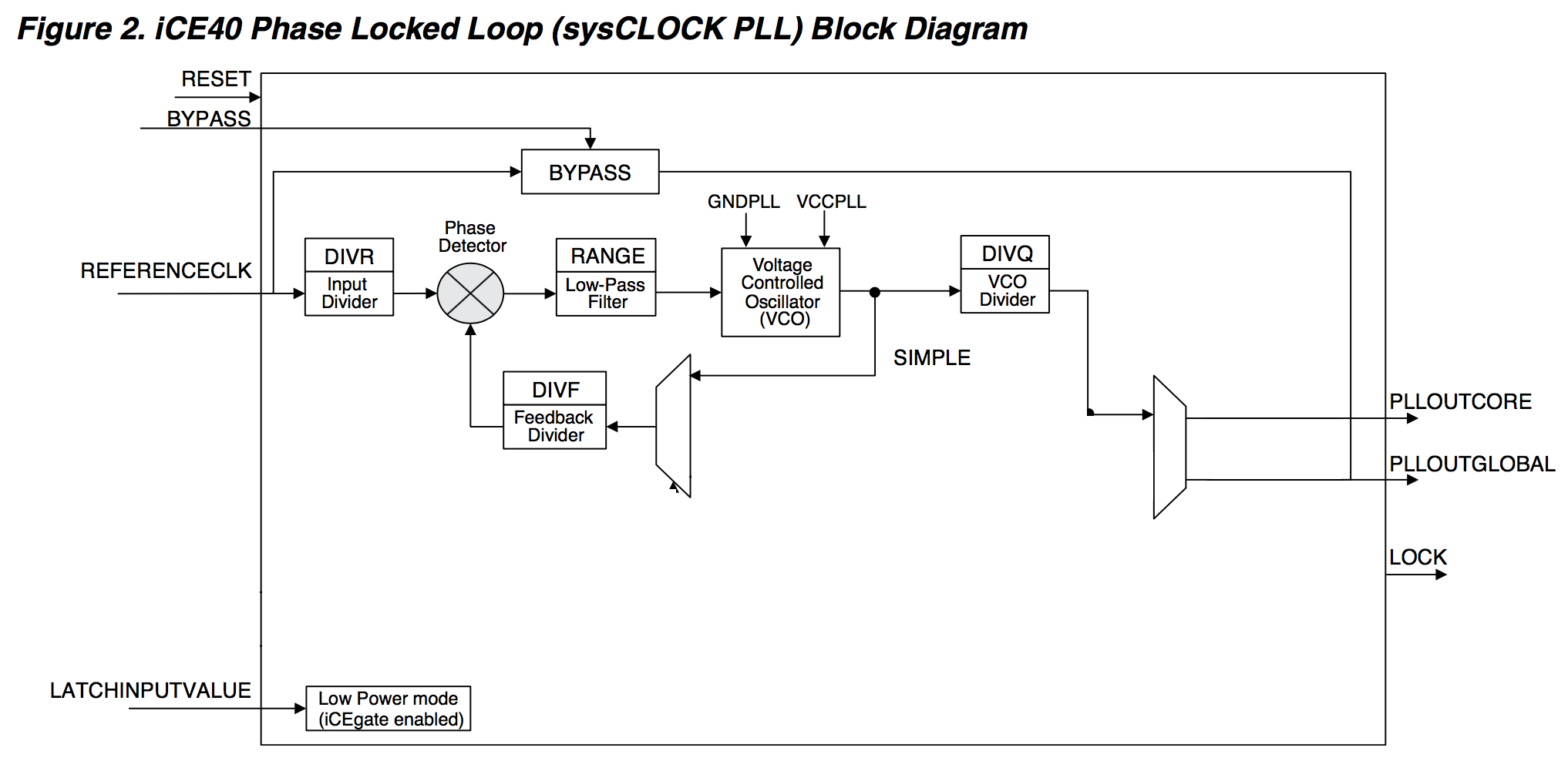
Here's the SIMPLE block diagram again:

We see not one but two outputs: PLLOUTCORE and PLLOUTGLOBAL.
Here's what the design and usage guide says about that:
-
PLLOUTGLOBALOutput from the Phase-Locked Loop (PLL). Drives a global clock network on the FPGA.
-
PLLOUTCOREOutput clock generated by the PLL, drives regular FPGA routing. The frequency generated on this output is the same as the frequency of the clock signal generated on the
PLLOUTLGOBALport.
The ICE40 FPGA has two kinds of wires:
- the regular, core, network that is used to wires different logical cells to eachother. The wire are short, but can be configured to be connected to eachother, and they are very flexible.
- 8 global networks. These 8 wires each cover the full chip.
The place-and-route tool will typically use global networks for wires that have the highest fanout (=number of endpoints). And one of the most obvious nets for those are clocks and resets.
The sb_pll40_core directory contains the pll.v that was originally created by icepll.
We see that clock_out is connected to PLLOUTCORE:
SB_PLL40_CORE #(
		.FEEDBACK_PATH("SIMPLE"),
		.DIVR(4'b0100),		// DIVR =  4
		.DIVF(7'b0101111),	// DIVF = 47
		.DIVQ(3'b101),		// DIVQ =  5
		.FILTER_RANGE(3'b010)	// FILTER_RANGE = 2
	) uut (
		.LOCK(locked),
		.RESETB(1'b1),
		.BYPASS(1'b0),
		.REFERENCECLK(clock_in),
		.PLLOUTCORE(clock_out)
		);
Go up one directory, edit the Makefile to select the right example, and type make.
Arachne-pnr says the following:
promote_globals...
  promoted u_blink_pll.clk, 25 / 25
  promoted 1 nets
    1 clk
  1 globals
    1 clk
In other words, arachne is smart enough to upgrade the generated clock u_blink_pll.clk to a global net, but
it still means that there is now a tiny bit of additional routing and timing uncertainty to go from PLLOUTCORE to
the global net.
In the sb_pll40_core_global directory, clock_out is now connected to PLLOUTGLOBAL.
Arachne shows this:
promote_globals...
  promoted 0 nets
  1 globals
    1 clk
There's now a straight connection between the PLL and the global net!
The Design and Usage Guide is not very comprehensive about how to make maxmimum use of the PLL, even in SIMPLE mode.
For that, we grab the ICE Technology Library and turn to the PLL Primitives section.
It turns out that the ICE40 PLLs can be instantiated as 5 different primitives! For now, let's look only at two of them:
- SB_PLL40_CORE
The SB_PLL40_CORE primitive should be used when the source clock of the PLL is driven by FPGA routing i.e. when the PLL source clock originates on the FPGA or is driven by an input pad that is not in the bottom IO bank (IO Bank 2).
- SB_PLL40_PAD
The SB_PLL40_PAD primitive should be used when the source clock of the PLL is driven by an input pad that is located in the bottom IO bank (IO Bank 2) or the top IO bank (IO Bank 0), and the source clock is not required inside the FPGA.
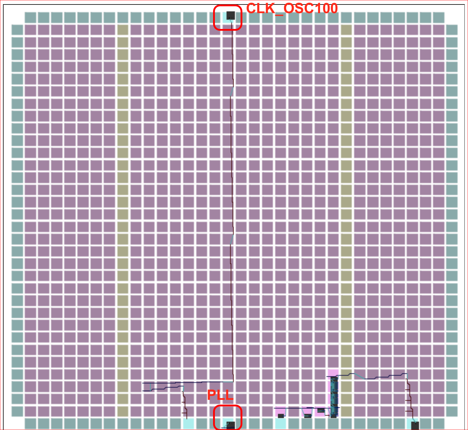
icepll uses the SB_PLL40_CORE, and that seems to work fine in practice. But if you look at the post-routing layout of
the design, you get the following:

The CLK_OSC100 pin and IO pad is at the top of the die but the PLL is located right across the chip, at the bottom.
In iCE40 HX8K Overview, you can read about the gory details of our FPGA, and learn that there one PLL at the top (location 16,33, right were our CLK_OSC100 is located) and one at the bottom (location 16,0).
It would have been much more obvious to have a straight connection from the CLK_OSC100 IO to the PLL, but somehow Arachne
didn't do that. The reason is that the SB_PLL40_CORE expects to be connected to a local net. It can't be driven directly from
an IO pad. But if you use a PLL, the input IO pad in which it is located can only be used for a straight IO pad to PLL connection.
The input can not be connected to a local net.
So arachne's only choice is to go from CLK_OSC100 input -> local net -> PLL at the other side.
Let's now look at pll.v of the sb_pll40_pad example:
SB_PLL40_PADS #(
                .FEEDBACK_PATH("SIMPLE"),
                .DIVR(4'b0100),         // DIVR =  4
                .DIVF(7'b0101111),      // DIVF = 47
                .DIVQ(3'b101),          // DIVQ =  5
                .FILTER_RANGE(3'b010)   // FILTER_RANGE = 2
        ) uut (
                .LOCK(locked),
                .RESETB(1'b1),
                .BYPASS(1'b0),
                .PACKAGEPIN(clock_in),
                .PLLOUTCORE(clock_out)
                );
There are 2 changes:
- SB_PLL40_CORE has been replaced by SB_PLL40_PAD
- REFERENCECLK(clock_in) has been replaced by PACKAGEPIN(clock_in)
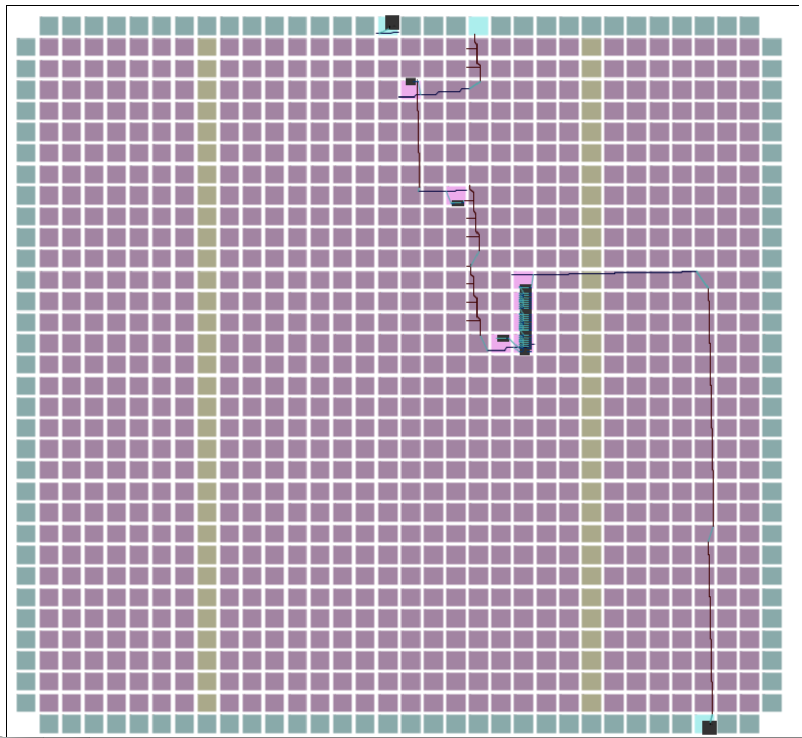
And here's the post-routing layout:

Unfortunately, the layout viewer doesn't really show the actual PLL, but it's clear now that everything interesting now happens at the top. And detailed placement reports confirm that the top PLL is indeed used.
The layout viewer only shows local routing, and we still see some black wiring at the location of pin CLK_OSC100. That's
because the example uses PLLOUTCORE.
Putting everything together, we get the sb_pll40_pad_global example,
which uses the _PAD PLL primitive and the PLLOUTGLOBAL output.
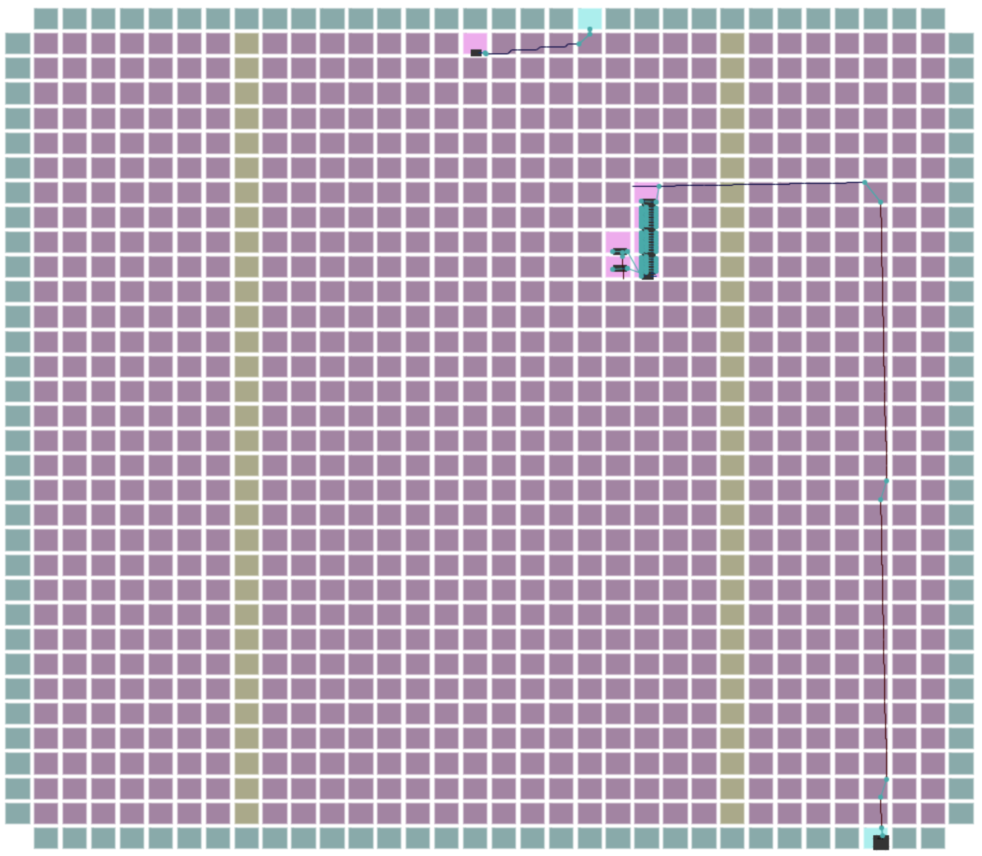
The layout looks like this:

For a design with the BlackIce-II board that just needs a single clock that is different than 100MHz, sb_pll40_pad_global is the
optimal solution!
What if we want to multiple PLLs in one design? Or maybe we need a a clock that runs at a certain speed and another one that runs at half the speed?
This will be discussed in PLLs Advanced.